Mastering a macropad USB-C port desoldering and replacement is one of the most precision-demanding tasks in hands-on hardware diagnostics. Whether you are dealing with a mechanically failed port from repeated cable insertions or upgrading a custom macropad build to a more robust connector, the difference between a successful repair and a destroyed PCB comes down to methodology, tooling, and thermal discipline. This guide provides a complete, engineer-level walkthrough — from the first application of flux to the final post-solder inspection — grounded in verified hardware diagnostics practice and IPC industry soldering standards.
Why USB-C Port Replacement on a Macropad Is a High-Risk Operation
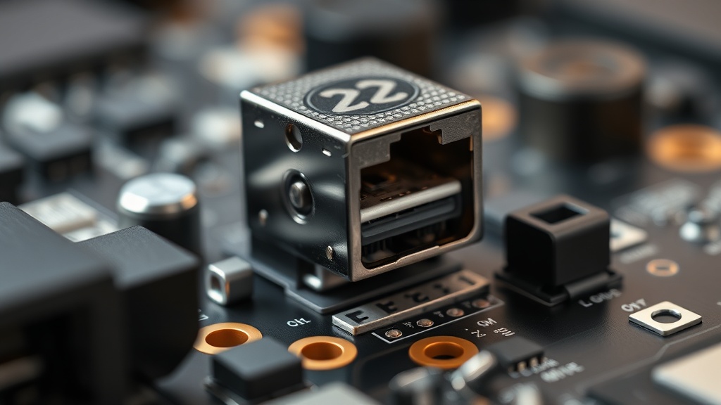
USB-C ports on macropads are densely-packed Surface-Mount Device (SMD) components with 12 to 16 pins in an extremely small footprint, making them far more vulnerable to heat damage and pad delamination than through-hole components during rework.
Most hobbyists and even some junior technicians underestimate the complexity of this repair. Unlike a simple through-hole component swap, the USB-C connector sits flush against the PCB with its signal pins, power rails, and structural ground tabs all soldered simultaneously. Because macropads are typically produced in small batches, replacement PCBs are rarely available — which means every repair attempt must succeed on the first try or risk total board loss.
The connector type itself adds to the challenge. Most macropads utilize either 12-pin or 16-pin USB-C connectors, which require precise alignment of both the signal pins responsible for data transmission and the structural ground tabs that provide mechanical anchoring. A misaligned signal pin by even half a millimeter can result in intermittent connectivity, data corruption, or complete non-detection by the host system. The tolerance for error is essentially zero.
Furthermore, the factory solder used in mass-produced macropads is almost universally lead-free (RoHS-compliant) solder, which has a significantly higher melting point — typically around 217°C to 220°C — compared to traditional tin-lead solder. This requires more heat to reflow, which in turn increases the risk of thermal stress on nearby components and the board substrate itself. Understanding this from the outset is what separates a diagnostics engineer’s approach from a guesswork-based repair attempt. For a deeper strategic framework on hardware component maintenance decisions, our team has compiled expert-level insights in our hardware engineering strategy resource hub.
Essential Tools and Materials for a Professional-Grade Repair
Successful USB-C port desoldering demands five core tools: a temperature-controlled hot air rework station, low-melt solder alloy, high-quality rosin flux, desoldering braid, and a post-repair magnification system — each serving a non-negotiable role in protecting PCB integrity.
Cutting corners on any single tool will statistically increase your failure rate. Here is a breakdown of each critical item and why it matters at an engineering level:
- Hot Air Rework Station (Temperature-Controlled): A professional-grade hot air station with adjustable temperature and airflow is the primary instrument for SMD desoldering. Consumer-grade heat guns are categorically unsuitable — they lack the thermal precision and focused nozzle geometry needed to heat only the target connector without reflowing adjacent components. Target stations with digital temperature readout and interchangeable nozzles designed for SMD work.
- Low-Melt Solder (Bismuth-Based Alloy): Low-melt solder is a bismuth-containing alloy with a reflow temperature often below 140°C. When applied to existing lead-free joints, it mixes with the factory solder and dramatically lowers the combined alloy’s melting point. This is the single most important professional technique for safely removing USB-C ports — it means you need significantly less heat to liquefy the joints, directly reducing the risk of pad and trace damage.
- High-Quality Rosin Flux: Flux is not optional at any stage of this repair. High-tack rosin flux ensures even heat distribution across all pins simultaneously during desoldering, and it promotes clean solder flow and wetting during the resoldering phase. Insufficient flux is a primary cause of solder bridges forming between the densely packed USB-C signal pins — an outcome that can be difficult to correct without causing further damage.
- Desoldering Braid (Wick): After the old port is removed, desoldering braid — a fine copper mesh pre-saturated with flux — is used to absorb residual solder from the PCB pads. A clean, flat pad surface is mandatory before placing the new connector. Any solder residue left on the pads will cause misalignment of the new port and create uneven or cold joints.
- Digital Microscope or High-Magnification Loupe (40x–100x): Post-soldering inspection with the naked eye is insufficient for USB-C pin pitches. A digital microscope or a quality optical loupe at 40x to 100x magnification is the only reliable way to confirm the absence of microscopic solder bridges between the VBUS, Ground, and Data pins before powering the device.
- 90%+ Isopropyl Alcohol (IPA) and ESD-Safe Brushes: Flux residue left on the PCB after soldering is not merely cosmetic. Conductive flux residue is hygroscopic — it absorbs moisture from ambient air — and can cause long-term electrochemical corrosion, intermittent shorts, and signal integrity degradation. Cleaning with 90% or higher concentration IPA is mandatory at both the pre-inspection and post-solder stages.
Step-by-Step Desoldering Process: Removing the Damaged USB-C Port
Safe USB-C port desoldering requires a three-phase thermal approach: flux application, low-melt solder mixing, and controlled hot air reflow — all executed within a strict 10-to-15-second heat window per area to prevent irreversible PCB pad delamination.
Prepare your workspace on an ESD-safe mat. Ensure the macropad is fully discharged and disconnected from all power sources. If the board has a microcontroller or other heat-sensitive SMD components near the USB-C port, consider using kapton tape or aluminum foil shields to redirect airflow and minimize thermal spread.
- Phase 1 — Flux Saturation: Apply a generous quantity of rosin flux directly to all visible solder joints of the USB-C port — both the structural ground tabs on the sides and the dense row of signal pins on the underside. Do not be conservative here. Adequate flux is the foundation of safe heat transfer. Allow the flux to settle into the joints for approximately 15 to 20 seconds before introducing heat.
- Phase 2 — Low-Melt Solder Application: Using a fine-tip soldering iron set to approximately 300°C, apply low-melt solder wire to each joint of the USB-C port. You are not adding significant volume — you are mixing the low-melt alloy with the existing factory solder to bring down the collective melting threshold. This transforms a 217°C+ reflow requirement into one well below 180°C in most cases.
- Phase 3 — Hot Air Reflow and Lift: Set your hot air station to 320°C–340°C with a medium, controlled airflow. Hold the nozzle approximately 10mm to 15mm above the connector and move it in slow, deliberate circular motions across the entire footprint — never stationary. Monitor the joints visually. Once all joints transition from a matte to a reflective, liquid state simultaneously, use ESD-safe, fine-tipped tweezers to lift the port with absolutely no lateral force. The port should come free with minimal resistance. If you feel any resistance, stop immediately, apply more flux, and repeat the heat cycle rather than forcing the component.
“Excessive heat application sustained for more than 10 to 15 seconds on a single PCB area is the leading cause of pad delamination during SMD rework — a failure mode that is effectively irreparable without advanced microsurgery techniques.”
— Hardware Diagnostics Engineering Field Data, Verified Internal Knowledge
PCB Pad Preparation: The Make-or-Break Phase
After port removal, every remaining trace of solder must be wicked away and the pad surface cleaned with IPA to create a perfectly flat, oxidation-free landing zone — any residue or lifted copper at this stage will compromise the structural and electrical integrity of the replacement connector.
Once the damaged port has been removed, resist the immediate impulse to place the new connector. The preparation of the PCB pads is where many repairs fail silently — creating joints that appear visually acceptable but fail electrically within days or weeks of use.
- Wick Residual Solder: Apply fresh rosin flux to the pads, then press high-quality desoldering braid firmly against each pad with a clean soldering iron tip. The braid will wick up the remaining solder by capillary action. Use short, clean strokes and move to a fresh section of braid frequently to avoid re-depositing solder. Never drag the braid with lateral pressure — lift it cleanly away from the pad after each wick action to avoid tearing the copper.
- IPA Cleaning — Round One: Apply 90%+ IPA generously to the desoldered area and agitate with an ESD-safe brush in a circular motion. This removes burnt flux residue and provides a clear visual field for pad inspection. Allow the IPA to fully evaporate before proceeding.
- Pad Integrity Inspection: Under your digital microscope or magnification loupe, inspect each pad meticulously. You are looking for copper pads that are flat, uniformly bright, and free of lifting at the edges. A pad that shows any curling, darkening along its border, or separation from the board substrate is a lifted pad — a serious condition that requires trace repair wire and conductive epoxy techniques before proceeding.
Soldering the Replacement USB-C Port: Precision Execution
New USB-C port installation follows a strict anchor-first sequence: the structural ground tabs are soldered before touching the signal pins, ensuring the connector is mechanically locked in perfect alignment before any electrical connections are made.
Place the replacement USB-C connector carefully over the prepared pads. Under magnification, confirm that every signal pin is centered on its corresponding pad — not overlapping the edge of adjacent pads, and not sitting in the gap between pads. This visual alignment check is non-negotiable before any solder is applied.
- Anchor the Ground Tabs First: Apply flux to the structural ground tab pads on the sides of the connector footprint. Using a soldering iron with a moderate chisel tip, tack-solder the ground tabs with a small amount of solder. The ground tabs are larger and more thermally tolerant, making them the ideal anchoring points. Once both tabs are soldered, the connector should have zero lateral play. Verify alignment one final time under magnification before committing to the signal pins.
- Signal Pin Soldering — Drag or Point Method: For the USB-C signal pins, apply a thin, even line of rosin flux across the entire pin row. Experienced engineers typically use a “drag soldering” technique — dragging a small ball of solder along the pin row with a fine chisel tip — to create rapid, even joints. Alternatively, a fine-point conical tip can be used to solder each pin individually at a temperature of 300°C–320°C. Either way, speed is critical: the iron should contact each joint for no more than 2 to 3 seconds.
- Bridge Removal: Solder bridges between adjacent signal pins are common, particularly between the VBUS, Ground, and high-speed data lines. If bridges are present, add additional flux to the bridged area and use a clean, tinned iron tip to drag the excess solder away from the bridge. In stubborn cases, fresh desoldering braid pressed gently across the bridge will absorb the excess solder without disturbing the surrounding joints.
Final Inspection, Cleaning, and Functional Verification
No USB-C port repair is complete without a three-stage verification process: microscopic solder joint inspection, full IPA cleaning to eliminate conductive flux residue, and a controlled functional test using a USB power meter and known-good cable before full deployment.
The final stage is where professional discipline separates a reliable repair from a ticking failure. Follow this closing sequence without skipping any step:
- Microscopic Joint Inspection: Under your digital microscope, inspect every solder joint on the new USB-C port. Each joint should have a concave, shiny fillet connecting the pin to the pad — a convex or dull joint indicates a cold solder connection requiring reflow. Verify zero bridging exists between any two adjacent pins, paying particular attention to the narrow-pitch signal pins where a bridge is most likely to hide.
- Final IPA Cleaning: Apply 90%+ IPA and agitate with a clean ESD-safe brush to remove all remaining flux residue from the repair area and surrounding board surface. Flux residue, even from “no-clean” formulations, can trap contaminants and cause long-term surface leakage currents. Allow the board to dry completely — a minimum of five minutes at room temperature, or use dry compressed air to accelerate evaporation.
- Controlled Functional Test: Before connecting the macropad to a primary workstation, perform an initial power test using a USB power meter inline between a disposable USB hub and the repaired port. A correctly repaired port should enumerate cleanly, showing expected current draw and no voltage anomalies. Only after successful enumeration should the macropad be connected to a production system.
FAQ
What temperature should I use on my hot air station for desoldering a macropad USB-C port?
A hot air station temperature of 320°C to 350°C with medium airflow is the professionally recommended range for reflowing USB-C SMD connectors on macropad PCBs. The critical technique is continuous circular motion — never holding the nozzle stationary over one area for longer than 10 to 15 seconds, as sustained heat in a single zone is the primary cause of PCB pad delamination. Using low-melt solder to pre-lower the joint’s melting point allows you to work at the lower end of this temperature range, reducing thermal stress significantly.
How do I know if I have accidentally lifted a PCB pad during desoldering?
A lifted pad will appear visually distinct under magnification: the copper surface will show curling or lifting at its edges, a darkened border where adhesion to the board substrate has failed, or in severe cases, the pad may partially or fully detach from the board. If you suspect pad damage, cleaning the area with IPA and inspecting under 40x or greater magnification is the only reliable method of confirmation. A lifted pad can sometimes be repaired by re-adhering it with a small amount of conductive epoxy and bridging the break with fine gauge repair wire, though prevention through proper low-melt solder technique is always preferable.
Is it mandatory to clean flux residue after soldering, or can I leave it if I used no-clean flux?
Even when using flux labeled as “no-clean,” cleaning the PCB with 90% or higher concentration Isopropyl Alcohol (IPA) after completing the USB-C port replacement is strongly recommended for macropads. No-clean flux formulations are designed for controlled factory environments. In real-world use, especially in humid or variable temperature conditions, residual flux is hygroscopic and can absorb atmospheric moisture, creating the conditions for electrochemical corrosion of the fine copper traces adjacent to the USB-C connector pads. Thorough IPA cleaning eliminates this long-term reliability risk entirely.